4 Discrete-Time Delta-Sigma Modulator
5 System Overview
Concept Engineering of Mixed Signals and Systems

We all live in an analog world where all we percieve is analog in nature but at the same time our technology process on digital data. We have sensors as input nodes. They can be voice signals, RF signals, pressure. temperatur, etc. Every system acquires the analog data and results in analog data which is called as actuators such as Speakers, etc. So the point is we need something which converts the data from analog domain to discrete or digital domain and again converts back to analog domain. Here comes the concept of Data Converters.

Figure 5.2 tells us that we have Continuous Domain where a signal can be represented as continuous in time and continuous in amplitude and Discrete Domain where the signal can be represented as discrete in time and amplitude. By sampling we discretise the signal from continuous time to discrete time and then by quantizing it we discretise its amplitude.
Our main focus will be on the design of Analog to Digital Converter
6 Block Level Representation

Acccording to Figure 12.4, We have a system where we have ADXL335 accelerometer as our analog sensor and we need to process the data on microcontroller so we need an ADC which takes the analog output from ADXL335 and provides the data in discrete form to the microcontroller. Considering the type of output provided by the accelerometer, we need to design low voltage, low speed, single-bit \(\Delta\Sigma\) modulator followed by a decimation filter. Our main focus will be on designing a second order single-bit \(\Delta\Sigma\) modulator using discrete time switch capacitor circuit.
Before diving deep into the circuit level, let’s look at our target specifications.
| Parameter | Symbol | Value | Units |
|---|---|---|---|
| Signal Bandwidth | \(f_B\) | 512 | kHz |
| Sampling frequency | \(f_{s}\) | 220 | kHz |
| Signal-to-Noise Ratio | \(SNR\) | 98 | dB |
| Supply voltage | \(V_{dd}\) | 1.5 | V |
6.1 NTF Selection

The matlab code creates an NTF (see Figure 6.2) with CIFB topology and performs dynamic scaling using the functions of \(\Delta\Sigma\) toolbox (see (tb-CIFB-params?))).
| Parameter | Value |
|---|---|
| a(1) | 0.2636 |
| a(2) | 2.137 |
| b(1) | 0.2636 |
| c(1) | 0.3097 |
| c(2) | 5.7837 |
While designing NTF, OSR, quantization levels[N] are fixed attributes and order of the modulator, out-band gain[OBG], cut-off frequency, etc are the iterative factors. Let’s discuss some facts about NTF and Quantizer.
\(Dynamic Range = SQNR =\frac{signal power}{noise power}\)
and in \(d\beta\), \(Dynamic Range =6.02 N + 1.76\) (where N = quantization levels)
as we decrease N by 1, SQNR decreases by factor of 6 \(d\beta\) and this can be fixed easil by increasing OBG. The working is quantizer is basically we need to compare the output from the loop filter against a bunch of levels and generate PWM quantity which is dependent on these levels. Hence, fewer the levels of quantizer, easier is the design of quantizer. So we try and reduce the number of levels as much as possible and the lowest we can go is 2 levels resulting in 1-bit quantizer. Clearly, we are pushing the assumptions we made in the mathematical analysis of quantizer too much for e.g. the realization of quantizer as white additive noise is only valid when the levels are more.
It turns out that for a single-bit modulator, the noise is still shaped out but since we have only two levels, technically speaking, the quantizer is always either in upper saturation or lower saturation. Also it is not answerable defining the gain of the quantizer.
This gives rise to an Empirical rule: Lee’s Rule which says that the NTF’s out-band gain (OBG) must be \(\le 1.5\). Whole bunch of simulations were run on 1-bit modulator and proven that Lee’s Rule will somehow make all the mathematical assumptions for quantizer hold true.
The mathematical assumptions are as follows:
- We treat quantization noise as ‘white’, ‘broad-banded’ and independent of input signal
- The error is bounded and also uniformly distributed between \([-\frac{\Delta}{2}, \frac{\Delta}{2}]\) (where\(\Delta\) = step size of quantizer)
As we are desiging a second order single bit \(\Delta\Sigma\) modulator, quantization level[N] = 2 and the NTF is being automatically designed using \(\Delta\Sigma\) toolbox

Figure 12.2 shows that we need discrete time integrators for our loop filter, 1-bit quantizer and 1-bit feedback.
7 Realisation of discrete time second order switch capacitor circuit

If we want to realize any discrete time transfer function H(z), we need a. discrete time switch-capacitor amplifier and b. discrete time switch capacitor integrator. Figure 7.1 shows the integrator in continuous time where the area under the curve shows the integrated output at any time instant ‘t’ and its equivalent in discrete time where the output at sample ‘n’ is sum of all samples till that sample. But now we have two possibilities:
- we sum up all the samples excluding the current sample. Where we get a transfer function as follows;
\[ V_{out}[n] = \sum_{m=0}^{n-1} V_{in}[m] \]
- we sum up all the samples including the current sample. Where we get a transfer function as follows;
\[ V_{out}[n-1] = \sum_{m=0}^{n-2} V_{in}[m] \]
Now, writing \(V_{out}[n]\) in terms of \(V_{out}[n-1]\),
\(V_{out}[n] - V_{out}[n-1] = V_{in}[n-1]\) this yeilds,
\(V_{out}[n] = V_{out}[n-1] + V_{in}[n-1]\) for case (a) where the current sample is excluded giving us a Transfer function: \(H(z) = \frac{z^{-1}}{1-z^{-1}}\). This gives us the ‘Delayed Switch-Capacitor Integrator’
and if we include the current sample then we have, \(V_{out}[n] = V_{out}[n-1] + V_{in}[n]\) giving us a Transfer function: \(H(z) = \frac{1}{1-z^{-1}}\). This gives us the ‘Non-Delayed Switch-Capacitor Integrator’
7.1 Implementation of Delayed Switch-Capacitor Integrator
So essentially, the equation speaks that we are storing the output and adding the input to the existing output. Therefore, to store the output we need a capacitor \((C_1)\), and we want to process this voltage onto the next capacitor \((C_2)\), but we also need to make sure that no current is being derived from it. Thus, we need to use a voltage controlled voltage source (Op-amp) but while designing on IC level, mosfets are always current sources controlled by voltage and its better to use OTA instead of Op-amps in our design. So, we need an OTA.
?fig-phis shows that in phase1, \(C_1\) will store the charge from \(V_{in}\) and in phase2, the charge will be transfered to \(C_2\) and it will store charge from previous sample. To put this together (see ?fig-Club)


Now, we also need to take charge injection into consideration and implement bottom plate sampling. Our derived switch-capacitor integrator will be having a Transfer function: \(H(z) = \frac{C_1}{C_2}\frac{z^{-1}}{1-z^{-1}}\) (See Figure 7.2)

The input is sampled in track phase \(\phi_1\) and transferred to \(C_2\) in hold phase \(\phi_2\) again in next \(\phi_1\), new \(V_{in}\) is sampled and hence, the sampled signal is available at output after one cycle proving the delay. (see Figure 7.3)

This boils down to a second order switch capacitor circuit follwed by a single bit quantizer as shown in Figure 7.4.

8 Capacitor Sizing
The capacitance ratio in the first stage can be computed using \[ a_1 = \frac{C_1 V_{\text{ref}}}{C_2} = \frac{C_1 V_{\text{dd}}}{C_2} \]
The absolute value of C1 is determined by a thermal noise constraint. The meansquare noise voltage yielding an SNR of 101 dB (98 dB plus 3 dB margin) relative to the power of a full-scale sine wave is \[ \overline{\nu_n^2} = \frac{(V_{dd}/2)^2/2}{10^{SNR/10}} = \frac{(0.75)^2/2}{10^{(101/10)}} = (22.3\,\mu V)^2 \]
The in-band input-referred mean-square noise voltage associated with the first integrator is approximately \[ v_n^2 = \frac{kT}{OSR \cdot C_1} \]
The \(c1\) coefficient specifies the weighting factor connecting the first integrator to the second
\[ c_1 = \frac{C_3}{C_5} \]
\(a_2\) is related to the feedback capacitor \(C_4\) and the 1-bit DAC’s differential reference voltage via following equation and setting \(C_4 = 0.1\) picofarrad arbitraryly
\[ a_2 = \frac{C_4 V_{dd}}{C_5} \]
This matlab code yeilds the capacitor values according to the desired equations as follows:
| Parameter | Value | Units |
|---|---|---|
| C_1 | 0.3 | pF |
| C_2 | 2.06 | pF |
| C_3 | 0.21 | pF |
| C_4 | 0.1 | pF |
| C_5 | 0.7 | pF |
9 OTA design for Switch Capacitor integrators
As we now enter on IC design level, we need to implement the discrete time integrator using CMOS elements. We will use Xschem for schematic entry and ngspice for simulation. The 130nm CMOS technology IHP-SG13G2 from IHP Microelectronics. Tools and PDK are integrated in the IIC-OSIC-TOOLS Docker image. This PDK is open-source, and the complete process specification can be found at SG13G2 process specification
9.1 Deriving required parameters for design
As mention in Chapter 7 the load driven by our circuit is purely capacitive and hence taking consideration of swing over gain, Folded Cascode topology (see ?fig-OTA) is what best suited in our case, where we have PMOS input pair.

Detailed analysis of Folded Cascode topology can be accessed here. You can find the quantitative as well as qualitative analysis , noise analysis, offset / mismatch analysis.
9.1.1 Deriving \(I\)
As shown in Figure 9.1 the magnitude of the output current under these conditions is \(I\), where \(I\) is the bias current in each half of the differential pair. (\(I\) is also assumed to be the standing current in the output cascodes.) Clearly, \(I\) must be large enough to transfer the charge from the input capacitor(s) to the integrating capacitor in the allotted time.(S. Pavan and Temes 2017)
Let’s allocate half of a clock phase (i.e., one quarter of a clock period) for slewing. Since the voltage on the left side of the input capacitor C1 can change by as much as \({{V_\mathrm{DD}}} = 1.5 V\) , we therefore need
\[ I > \frac{C_1 VDD}{T/4} = \frac{0.36 \, \mathrm{pF} \cdot 1.5 \, \mathrm{V}}{1.13 \, \mu\mathrm{s}} = 0.8 \, \mu\mathrm{A}. \]
9.1.2 Deriving \({g_\mathrm{m}}\) from Time-constant calculation
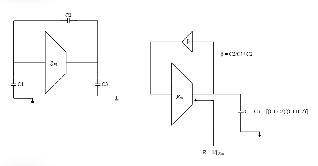
Figure 9.2 shows the small-signal model of an integrator in the charge-transfer phase and an equivalent circuit from which we see that the time-constant is
\[ \tau = RC = \frac{C_1 + C_3 + \frac{C_1 C_3}{C_2}}{g_\mathrm{m}} \]
Now let’s say we take the linera settling to provide attenuation of 100 \(dB\)
\[ \frac{T}{4} = \tau \ln(10^5) \approx 12\tau \]
This gives us \[ {g_\mathrm{m}} = \frac{C_1 + C_3 + \frac{C_1 C_3}{C_2}}{\frac{T}{48}} = 5.7 \, \mu\frac{A}{V} \]
9.1.3 Deciding \(L\) and \(W\) for MOSFETS
Now that we have the exact values for \({g_\mathrm{m}}\) and \({I_\mathrm{D}}\), we can derive the values of \(L\) and \(W\) by making use of \({g_\mathrm{m}}\)\({I_\mathrm{D}}\) vs \({I_\mathrm{D}}\)\(W\) curve. Refer to Chapter 10 for detailed discussion regarding sizing.
We already know the current flowing throught each MOSFET (See Figure 9.1). As shown in Figure 9.3 and Figure 9.4, by appropriately choosing the \(L\), we can obtain \(W\) for $ = 7.12 $
The minimum length consideration while designing in low voltage CMOS technology should be atleast 3 to 4 times the \(L_\min\). In our case \(L_\min = 0.13 \, \mu\).


9.1.4 OTA biasing using current mirror

Figure 9.5 explains the biasing of the OTA using Wilson’s current mirror topology.
9.1.5 Performance of designed OTA
For understanding how the designed OTA is performing, we run transient analysis, ac analysis and dc analysis. In order to achieve these analysis, we need to put our OTA in negative feedback loop (unity feedback loop in our case) and realize the plots. Figure 9.6 shows the transient plot and gives us the time constant in which it reaches the steady state. NgSpice yeilds tsettle = 8.663771e-09
Figure 9.8 and Figure 9.7 shows us the magnitude and phase over a range of frequency.Where NgSpice yeilds dc_gain = 9.156547e-01 fbw = 7.544229e+07 Gain_error = -8.41453e-02


10 Sizing using gm over Id method
Now that we have designed the topology of our OTA(refer to foldedCascode) and we already know the value of \(g_\mathrm{m}\), and \(I_\mathrm{D}\), we need to derive the widths \(W\) \(L\) and lengths of our design.
In nanometer CMOS, the MOSFET behavior is much more complex than these simple models. Also, this highly simplified derivations introduce concepts like the threshold voltage or the overdrive voltage, which are interesting from a theoretical viewpoint, but bear little practical use. Modern compact MOSFET models (like the PSP model used in SG13G2) use hundreds of parameters and fairly complex equations to somewhat properly describe MOSFET behavior over a wide range of parameters like width, length and temperature. A modern approach to MOSFET sizing is thus based on the thought to use exactly these MOSFET models, characterize them, put the resulting data into tables and charts, and thus learn about the complex MOSFET behavior and use it for MOSFET sizing.
The gm over Id methodology has the huge advantage that it catches MOSFET behavior quite accurately over a wide range of operating conditions, and the curves look very similar for pretty much all CMOS technologies, from micrometer bulk CMOS down to nanometer FinFET devices. Of course the absolute values change, but the method applies universally.
A brief is available here
10.1 Testbench for MOSFETSWEEP
In order to get all the operating points for lv nmos shown in Figure 10.1, and lv pmos shown in Figure 10.2, we run a techsweep and obtain curves related to parameters such as \({g_\mathrm{m}}\), \({g_\mathrm{ds}}\), \({C_\mathrm{gs}}\), \({I_\mathrm{d}}\), \({V_\mathrm{GS}}\), \({V_\mathrm{DS}}\), \(L\), \(W\). We create a testbench in Xschem which sweeps the terminal voltages, and records various large- and small-signal parameters, which are then stored in large tables.


After obtaining the parameters we plot them using Matlab, and obtain some important curves or graphs in order to understand the MOSFET’s behaviour.
11 Realisation of 1-Bit Quantizer
11.1 Designing of the 1-Bit Quantiser
Based on the collected experience in this lecture we are desiging a 1-bit Quantiser (Comparator) in Xschem.
11.2 Defining a Comparator
This block compares two input voltages, \({V_\mathrm{1}}\) and \({V_\mathrm{2}}\) and determines their relationship. If \({V_\mathrm{1}}\) > \({V_\mathrm{2}}\) output is set to \({V_\mathrm{DD}}\). Otherwise, if \({V_\mathrm{1}}\) < \({V_\mathrm{2}}\) the output is 0\({V_\mathrm{}}\).
The ideal input-output characteristics should resemble a signum function, as illustrated in ?fig-Ip_Op(Comp).
 {#fig-Ip_Op(Comp)}
11.3 Realising a Comparator
Consider an amplier with a sufficiently large gain. For simplicity consider one input \({V_\mathrm{in}}\), the output is going to be amplified by factor A. Amplifier operates between \({V_\mathrm{DD}}\) and GND. If the gain is large emough the output will saturate to \({V_\mathrm{DD}}\) or GND.
The minimum input required for the output to reach \({V_\mathrm{DD}}\) is \({V_\mathrm{DD}}\)/\(A\), at which point the comparator produces an output of \({V_\mathrm{DD}}\).
The output is then fed into a digital block, typically a flip-flop, to resample the obtained signal. For the flip-flop to register a digital 1, the amplifier’s output must exceed the input threshold voltage \({V_\mathrm{TH}}\).
As we know that the common implementation of first stage OTA is Differential Pair as shown in Figure 11.1.

The gain of the circuit, as shown in Figure 11.1 is given by: \({V_\mathrm{out}}\) = \({g_\mathrm{m}R}\)\(\Delta V\) Initially, the output of Figure 11.1 is zero. When an input is applied, the output gradually increases due to the influence of parasitic capacitances. Over time, it settles exponentially to its final value. The closed form expression for exponentially settling behaviour is given by: \[ V_{\mathrm{out}} = g_m R \Delta V \left(1 - e^{-t/\tau}\right) \]
To accelerate the response of the output curve, we need to adjust \({\tau}\) as its magnitude cannot be directly altered. One effective approach is to replace the resistor with a negative resistor, which helps achieve faster settling.
\[ -g_m R \Delta V \left(1 - e^{t/\tau}\right) g_m R \Delta V \left(1 - e^{t/\tau}\right) - {g_\mathrm{m}R}\Delta V \tag{11.1}\]
Equation 11.1 gives much quicker settling in the output.
Negative resistor is if we apply voltage we should not be drawing current but we should put the current in the node in order get negative reistance. We cannot have a constant current source because it should depend on \({V_\mathrm{t}}\) so we should use voltage control current source. Simplest voltage control current source is MOSFET. Therefore we replace resistors by PMOS’s as shown in Figure 11.2.
A negative resistor is characterized by the property that when a voltage is applied, it does not draw current but instead injects current into the node, effectively creating negative resistance. A constant current source cannot be used in this case, as the current must depend on \({V_\mathrm{t}}\). Therefore, a voltage-controlled current source is required. The simplest implementation of a voltage-controlled current source is a MOSFET. Consequently, resistors are replaced with PMOS transistors, as illustrated in Figure 11.2.

Initially, the output voltages \({V_\mathrm{x}}\) and \({V_\mathrm{y}}\) decrease as current is drawn from the top PMOS transistors. Among them, \({V_\mathrm{x}}\) drops more rapidly than \({V_\mathrm{y}}\). As \({V_\mathrm{x}}\) decreases, the current through its corresponding transistor increases, eventually surpassing the externally drawn current. As a result, \({V_\mathrm{y}}\) begins to rise. As \({V_\mathrm{y}}\) increases, the gate voltage at \({V_\mathrm{x}}\) also increases, reducing the current through the transistor. Consequently, the amount of current being pushed into the node becomes less than the current being pulled out, causing \({V_\mathrm{x}}\) to drop even further.
Ultimately, this feedback process leads to: \({V_\mathrm{y}}\) reaching to \({V_\mathrm{DD}}\) \({V_\mathrm{x}}\) reaching to 0\({V_\mathrm{}}\)
This kind of exponential increase is called “Regeneration”.
When \(\Delta V\) < 0, the voltage \({V_\mathrm{y}}\) should decrease while \({V_\mathrm{x}}\) should should rise to \({V_\mathrm{DD}}\). However, a challenge with this approach arises due to the positive feedback, which reinforces the voltages at \({V_\mathrm{DD}}\) and 0\({V_\mathrm{}}\). Once these values are established, the positive feedback works to maintain them, preventing a smooth transition.
In this configuration, the PMOS transistors remain in the same state, and the switching action relies on the two NMOS transistors. However, unless the current drawn from node \({V_\mathrm{y}}\) is significantly stronger, it cannot be effectively pulled down to 0\({V_\mathrm{}}\).
The key issue is that after completing a comparison for the previous input, the circuit retains the same output state while starting a new comparison. To ensure proper operation, both outputs must be reset before a new comparison begins.
The total time available is from 0 to \({T_\mathrm{s}}\) where, the first half is dedicated to sampling and the second half is allocated for regeneration.
The comparator operates in the regeneration phase, denoted as \(\phi c\) and in the sampling phase, represented a \(\overline{\phi c}\). During the sampling phase, the outputs can be reset. To achieve this, switches are used to reset the outputs to \({V_\mathrm{DD}}\) as in Figure 11.3.

In Figure 11.3, the two NMOS transistors do not need to be active during the reset phase of the PMOS transistors. Therefore, they can be turned off by switching off the bottom NMOS transistor. This allows the circuit to be clocked at \(\phi c\). Additionally, PMOS transistors can be used as switches for this operation as in Figure 11.4.

To describe the output behavior of a PMOS switch with respect to the clock signal \(\phi c\), here’s how it works step-by-step: 1.When \(\phi c\) = 0: The switches are off, so both The output of above Figure 11.4, \({V_\mathrm{x}}\) and \({V_\mathrm{y}}\) are at 0\({V_\mathrm{}}\). 2.When \(\phi c\) = 1: The switches are now on. Initially, \({V_\mathrm{x}}\) starts to drop faster because the PMOS transistor turns on when the voltage difference \({V_\mathrm{DD}}\)-\({V_\mathrm{TH}}\) is large enough. 3.As \({V_\mathrm{x}}\) drops and approaches a certain threshold, the PMOS turns on completely. The voltage at \({V_\mathrm{y}}\) then starts increasing and approaches \({V_\mathrm{DD}}\). Simultaneously, \({V_\mathrm{x}}\) continues to drop due to the action of the PMOS switch.
Issue with Static Power Consumption in Comparator Circuit
In the described PMOS-NMOS comparator circuit, the comparison process halts at a certain point where: \({V_\mathrm{y}}\) = \({V_\mathrm{DD}}\) and \({V_\mathrm{x}}\) = 0 At this stage, the NMOS transistor on the right side is turned on, which keeps the corresponding PMOS transistor in the ON state. Static Power Consumption: After the comparison is complete, and there is no change in the inputs and outputs, static power consumption persists. This is due to a direct path from \({V_\mathrm{DD}}\) to ground, as the NMOS remains on while the PMOS continues to conduct.
Influence of Differential Voltage(\({\Delta V}\)): When the differential voltage \({\Delta V}\) is large, the term \(\frac{\Delta V}{2}\) becomes significant. This results in ${V_} being very small, which in turn causes the PMOS transistor to turn off, effectively reducing power consumption. However, when the differential voltage \({\Delta V}\) is small, the voltage difference is insufficient to turn off the PMOS, allowing a direct path from \({V_\mathrm{DD}}\) to ground, and consequently leading to static power consumption.
To address this issue, a direct connection exists between the PMOS and NMOS transistors, creating an unintended path from \({V_\mathrm{DD}}\) to ground. To resolve this, an additional element should be introduced between points A and B, as illustrated in the diagram below Figure 11.5

The goal is to ensure that node B is OFF when \({V_\mathrm{x}}\) = 0 \({V_\mathrm{}}\) and node A is ON when \({V_\mathrm{y}}\) = \({V_\mathrm{DD}}\). This can be achieved by using an NMOS transistor, with its gate connected to \({V_\mathrm{x}}\) and \({V_\mathrm{y}}\) as shown in #fig-comp-1

In the diagram Figure 11.6, the drains and gates of the PMOS and NMOS transistors are connected to each other, forming a CMOS inverter.
Thi circuit is known as Strong-Arm Latch. Drawing it neatly as in ?fig-comp-final 
In practice there is one more modification made, along with ressetting X and Y we will also reset P and Q.
\({V_\mathrm{1}}\)-\({V_\mathrm{2}}\) = \({\Delta V}\) > 0
The output analysis of ?fig-comp-final is showin in Figure 11.7.
When, \(\phi c\) = 0, \({V_\mathrm{X,Y,P,Q}}\) = \({V_\mathrm{DD}}\) When, \(\phi c\) = ON, switches are OFF.

Figure 11.8 shows the transient analysis of our comparator.

11.4 Implementing a Strong Arm Latch for Delta-Sigma Modulator
Based on the above theory, we need to design a comparator and a latch that stores the output data from the comparator and converts it into a strong digital output.
(ig-comp2-sch?)- and Figure 11.10 shows the implementation and transient analysis of Strong Arm Latch Comparator respectively.


12 Clock Generator
Mixed-signal systems must balance elements that are critical in the digital domain as well as the analog domain. One important area of digital interface design in mixed-signal systems is clocking, which must be used to enforce timing between components and to read data from ADCs. Many mixed-signal systems operating in the low-to-moderate frequency range will use a reference oscillator, and there may be a need to synchronize multiple clocks across a system to accurately sample and synchronize the entire system.
In designing a sigma- delta ADC, we can say that the clock is the heartbeat of the ADC, synchronizing all operations. It means that the clock plays a crucial role in the overall system operation. The clock precisely controls the timing of various ADC components, and without it, neither sampling nor processing can occur.
let’s see clock’s role precisely:
1. Sampling Control:
The clock determines when the ADC should take a sample of the analog signal. In our system, the sampling frequency is 220 kHZ, meaning a new sample is taken every 4.545 seconds.
\[ T_s = \frac{1}{f_s} = \frac{1}{220 \times 10^3} = 4.545 \mu s \, \]
If the clock is too slow, insufficient data is captured, leading to signal degradation. If the clock is too fast, the circuit may not respond correctly, introducing noise and errors.
2. Control of the \(\Delta\Sigma\) Modulator Processing:
The \(\Delta\Sigma\) ADC operates using a feedback loop, which consists of: Integrators Comparator Flip-Flop
The clock synchronizes these components, ensuring the correct generation of the digital output.
Every clock cycle, the following steps occur: integrator updates its value. The integrator accumulates past values and combines them with the new input. This operation occurs once per clock cycle. Comparator determines if the new value is above or below zero. The comparator outputs a digital 0 or 1 at each clock edge. This output is directly sent to the digital processing stage. Feedback loop adjusts the input based on the digital output. The feedback system returns a digital signal to the integrator to correct conversion errors. If the clock is not properly configured, the modulator may malfunction, leading to incorrect digital output. If the clock is too fast, noise increases, and synchronization between analog and digital circuits is lost.
3. Flip-Flop Control and Comparator Decision-Making:
The comparator evaluates the integrator’s output and determines a digital 0 or 1 at each clock edge. Every time the clock triggers, a new digital value is stored, preparing it for further processing. The D Flip-Flop stores this digital value and generates the final bitstream. Without clock flip-flops store the data randomly and that is not the thing we want, because it leads to corrupt digital output.
4. Digital Filter (Decimation Filter) Control:
After the modulator, a digital filter (Decimation Filter) processes the high-speed output data. This filter, operating with the system clock and its divided versions, reduces the data rate to generate the final 16-bit digital output.
To design this \(\Delta\Sigma\) ADC clock, we must consider that we need two non-overlapping clock signals for proper operation. In a \(\Delta\Sigma\) ADC, capacitor switching and signal processing occur in two consecutive steps. One phase is used for sampling, while the other is used for integration and processing. If both clocks are high at the same time, it may cause signal interference and increased noise. To avoid this issue, two non-overlapping clocks are used, ensuring that they never go high simultaneously. The Sample-and-Hold circuit in an ADC requires two separate phases: In Phase 1, sampling takes place. In Phase 2, signal processing and data transfer occur. This circuits operation is based on charge transfer by switching. As shown by the time-domain waveforms in figure, during integrating phase ∅2, the charge stored in a sampling capacitor Cs is transferred to an integrating capacitor C1 of the switch. The discharging of Cs takes place at an exponentially decaying rate.
in switch capacitor circuits, the maintenance you should ensure is that the clocks never overlap.
12.1 Why non-overlapping phases?
1. Preventing short circuit current:
In switched-capacitor circuits, two switches are controlled by complementary clock phases. If both clock signals go high simultaneously, both switches turn on, creating a short circuit to ground or supply voltage. A non-overlapping clock eliminates this issue by ensuring a small delay (Dead Time) between the two clock phases.
2. Improving Sampling Accuracy:
In \(\Delta\Sigma\) ADCs, capacitors require sufficient time to charge or discharge before the clock phase changes. If the clock phases overlap, the capacitor may not fully charge, leading to sampling errors. A non-overlapping clock ensures accurate data transfer and minimizes noise.
3. Reducing Charge Injection & Clock Feedthrough:
Overlapping clock phases can cause charge injections and clock feedthrough, leading to signal distortion and increased noise. A non-overlapping clock helps to reduce these effects significantly.

12.2 How to Generate a Non-Overlapping Clock?
To generate ϕ1 and ϕ2 clock phases that never overlap, delay elements (RC delay, buffers, inverters) and AND/NOR gates are commonly used. The propagation delay is determined by the number and sizing of inverters in the non-overlapping circuit. While increasing the number of inverters extends the delay, it also increases power consumption and chip area. Transmission gates can be used alongside inverters to optimize delay and reduce the number of inverter stages. Switched capacitor circuits are widely used in ADCs, comparators, filters, and sample-and-hold circuits due to their compact and reliable design. The inverter chain configuration affects clocking sequences, where odd/even numbers of inverters generate specific logic transitions. Proper inverter sizing is crucial for achieving high-speed operation while minimizing area.
So, we saw that for example we don’t need 2 clocks to be high. At the same time phase 2 is going high after phase 1 is low by this you need logic to give you an output of 1 when both inputs are zero so that’s a NOR gate.
As you can see in the picture The basic non-overlapping clock generator consists of a S-R flip-flop, with inverters in series before the feedback, to add delay as required. Each sub-block contains inverters and one transmission gate to produce desired delay in the falling or rising edge.
.svg)
12.3 Schematic entry of Clock Generator
There is the design of the non-overlapping clock phases with our project specifications.


13 Final Design
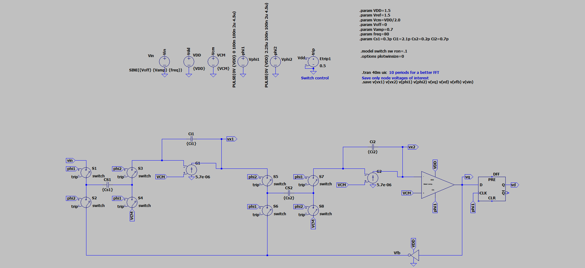
Figure 13.1 shows the schematic entry in LTSpice which acts as a reference to our circuit

Figure 13.3 is the output from LTSpice which is taken as reference. Figure 13.2 shows the implementation of real circuit , where the designed switch capacitor using OTA and comparator are put together in Xschem. vo1 representing the output from first integrator, vo2 from second integrator, and vcmp from the comparator, which then creates a feedback loop.
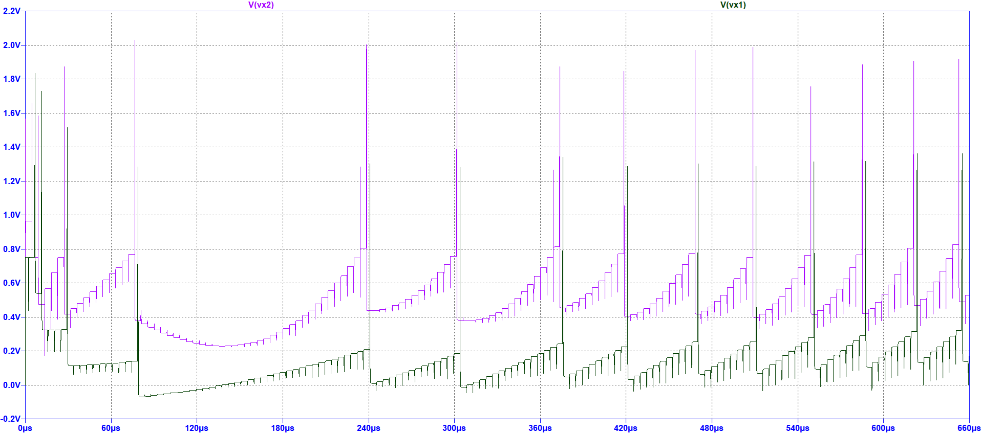

Figure 13.3 gives us the reference plot and Figure 13.4 is the output of our real circuit which portrays that the switch capacitor block is working perfectly fine as we can see the plot till \(60\mu\) in Figure 13.3 and compare it with Figure 13.4
We can further analyse the output behaviour of switch capacitor block by looking at the Figure 13.5.

The current status of the output from dsm is shown in Figure 13.6
