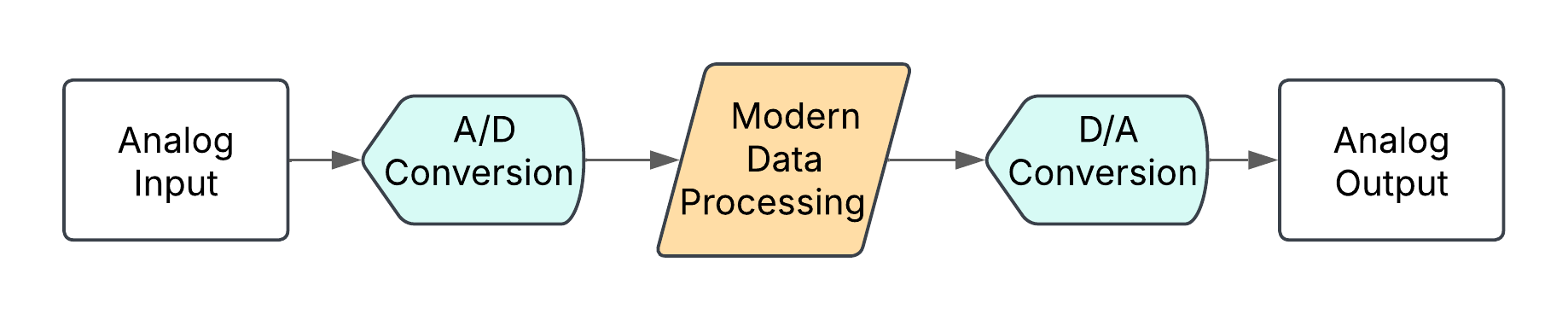
flowchart LR
  A[Anti-Alias Filtering] --> B[Sampling]
  B --> C[Quantization]
  C --> D[Digital Filtering]
6 Design of an Analog-Digital-Converter after the ADS1115
7 Introduction
Since more and more manufacturers are ending their production of integrated circuit solutions, the development of full custom solutions is becoming increasingly attractive. Thus, the different subgroups of the course “Concept Engineering Mixed-Technology Systems”, held by Professor Meiners at Hochschule Bremen, are tasked with the development of an Analog-Digital-Converter, roughly modeled in a way to replace the ADS1115 by Texas Instruments within a specified measurement system-chain.
Data conversion is a hot topic in the world of electronics. Most signal processing nowadays has shifted to the digital domain, due to the enourmous pace with which digital electronics have evolved in terms of speed and size, to the point where data rates in the Gigahertz range are becoming the norm, while the underlying semiconductor technologies continuously shrink to mere nanometers.
However, this does not change our analog world, nor the need to interface data from that domain into that of our “state-of-the-art” technologies. This consideration applies to all sorts of trackable or sensable data, of accustic, optical or mechanical nature. To fit into the evolving nature of the digital domain, converters should be able to keep up, regarding the speed, precision and reliability with which they interface.
For this reason, we shall attempt to outline one of the most popular ways to convert data given the technology of our time. The approach is that of the Sigma-Delta converter. In the following we present our approach to designing such an ADC. This includes a theoretical analysis of the workings of \(\Sigma \Delta\) ADC’s, an exploration of it’s basic behavioural characteristics on system-level, deriving basic and idealized circuits to match the behaviour, and lastly a detailed design of the established circuit-level system using SPICE simulations within the xschem design environment, where concrete solutions on IC-level will be proposed.
7.1 Top-Level Overview of Considered System
The considered system of interest for this semester is a classical meassurement system, consisting of an accelerometer as our analog data source, an ADC to convert said analog data to the digital domain, which can then be handled by a microcontroller as our processing unit.
The specific board-level components that are considered for this signal-chain are the ADXL335 accelerometer, the ADS1115 ADC and an ESP8266 microcontroller.
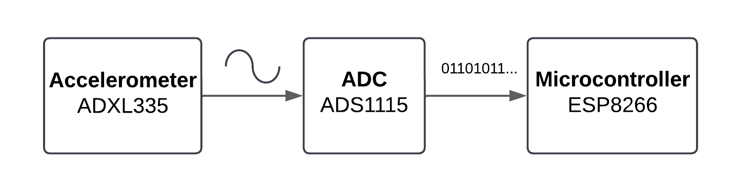
The mentioned ICs are given as evaluation- & breakout boards as part of the lab inventory.
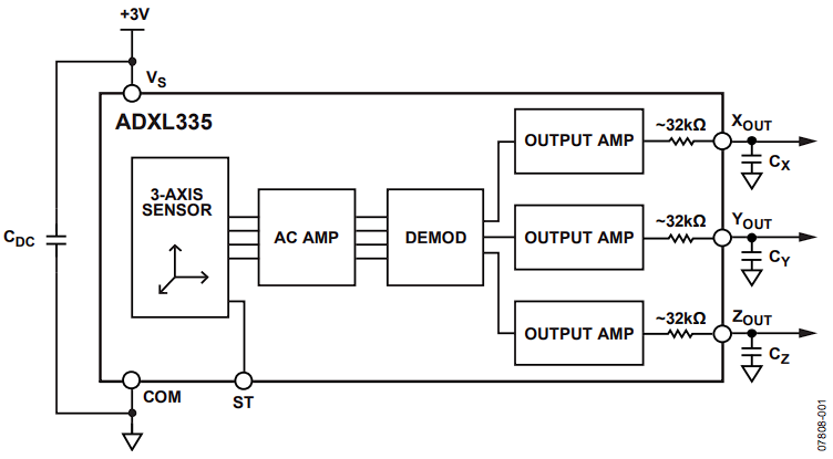
The accelerometer is a specific example of a micro electro-mechanical system (MEMS) used for the purpuse of sensing. This in essence utilizes capacitive Accelerometer, where the plates of that capacitor are within the internal structure, which allows for varying distances of the plates (or potentially “fingers”) resulting in a varying capacitance given an acceleration. The analog change in capacitance is what we will ultimately need to consider when it comes to system interfacing. (Fraden 2015)
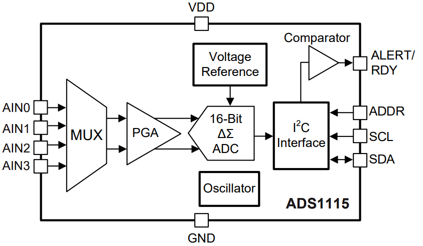
The ADS1115 is a Delta-Sigma ADC which includes various auxillary subsystems, like a multiplexer for the multiple input channels, an input programmable gain amplifier (PGA), an interface section to support the I2C communication protocol, etc.
The ESP8266 is a typical microcontroller, which allows us to measure data either directly through analog pins, which would utilize internal ADCs, or we can use the digital pins to utilize the full-fletched ADS1115 for the job of data conversion.
7.2 General Overview of given ADC
Figure 7.6 shows a more detailed block diagram of the ADS1115, which adopts informations from it’s datasheet (Instruments 2009). The focus of our work lies on the components in the orange box. The theory for the digital filter stage following the modulator is also briefly explored. The modulator itself comprises the switched capacitance to sample the input signal, an integrator (or accumulator) and the quantizing comparator to output a PWM signal. The other blocks depicted are considered auxillary block. These include the multiplexer which can be used to switch between different inputs. It is followed by a programmable gain amplifier. The amplification factor can be selected via an I2C interface which is also used to select the input channel, sample rate, as well as for the read out of the converted digital data among others. Since these auxillary blocks do not add to the functionality of the modulator itself it was decided to not explore them any further. In case of the reference oscillator and the voltage reference, these are modeled as ideal inputs during simulations.

8 Theory and Charactersitics of Delta-Sigma Modulators
8.1 Top-Level Overview
Delta-Sigma modulators (\(\Delta\Sigma\)) are generally speaking 1-bit sampling systems that utilize the principle of “oversampling”. To start this chapter of, we would like to briefly elaborate on some of the key elements of these modulator systems.
An ADC with respect to \(\Delta\Sigma\) modulator systems can be represented, using the following block diagram for the case of analog-to-digital conversion.
Anti-Aliasing measures have to be considered to ensure a “clean” input signal to the modulator system, without unwanted parasitic components.
The sampling then discretizes the input signal in time, before the quentization does the same with regard to its value (or amplitude).
The digital filtering is then responsible to transform the discrete signal into an output from which the original input can be extracted. This typically involves lowpass filtering, specifically utilizing a “moving-average” filter. In case of \(\Delta\Sigma\) modulators, which utilize oversampling, it also includes down-sampling/ decimating. The resulting data rate then most often resembles something close to the Nyquist rate of the signal band.
8.2 System overview of \(\Delta\Sigma\) Modulators
The modulator, which is a 1-bit sampling system, gets it’s name from two fundamental characteristics of it’s functionality.
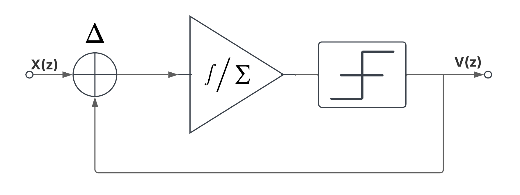
Figure 8.1 shows the fundamental block diagram of the modulator. The delta (\(\Delta\)) is realised through the fact that we take the difference between our input signal and the fed back signal from the output as our reference. Therefore we are not exactly sampling the input, but instead the difference/ delta between our input and our previous reference point.
The next fundamental block in an integrator, which in the discrete domain is also considered an accumulator or summator (\(\sum\)). Therefore, our established difference at it’s input is continuously summed up.
It is because of this that the system is characterizable as an “error accumulation structure”.
The result of that summation is then fed into a quantizer, which is realized through a 1-Bit ADC, which is in essence a comparator. this checks the incomming accumulator output at the defined high sampling rate and outputs either a ‘1’ or ‘0’, resulting in a 1-Bit datstream that resembles a pulse-width-modulated signal, correlated to the duration of the “rising” and “falling” slopes of the accumulator/ integrators outputs.
The resulting duty-cycle of the PWM-datastream will then be an indication for the inputsignal of the modulator. Assuming an initial condition of the quantizer output, an input level of zero would result in a \(\Delta\) that shifts between the two extremes of the quantizer, equally around 0. The integrator would therefore have equal slope speeds for both the rising and falling periods, leading to equal pulse lengths at the output.
In case of a non-zero input, e.g. positive, the high-pulses of the PWM will be longer, due to the integrator being fed with a “lower magnitude” of \(\Delta\) during this time, therefore showing a slower change at the output, compared to the complementary case.
The resultig PWM can then lead to valid representations of our input samples by utilizing digital filtering. As mentioned previously, we average a bunch of samples from the PWM datastream, using triangularly weighted coefficients within the filter structure, to get proper individal samples. Those in turn are then down-sampled to the requiered Nyquist rate.
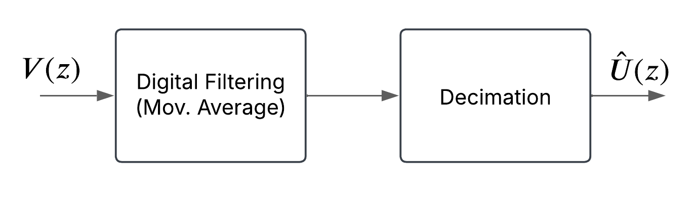
So summarized, the digital filtering will reduce high-frequency noise while passing the input signal to the output of the converter at a reduced data rate.
The reason why we oversampled in the first place, only to end-up with a lower datarate anyways, will be discussed in the next chapter.
8.2.1 Oversampling and Noise Shaping
Oversampling converters offer an alternative to the classical Nyquist-Converters. The latter utilize sampling rates that are either equal or slightly higher than the Nyquist-frequency of the system, meaning at least twice the required signal bandwidth \(f_B\), so that the input can be reconstructed reliably afterwards, according to the Nyquist-Theorem (in turn avoiding aliasing) (Schreier 2017). \[\begin{align} f_s \geq 2\cdot f_B \end{align}\]
Nyquist-converters generally suffer from the following aspects, limiting them in their potential to offer outputs with high resolution at decent speeds. They require a high degree of complexity and matching accuracy regarding their analog components for proper precision, which even than is still constrained. Those that can achieve high resolution, meaning a high number of effective bits (ENOB), need circuitries that ultimately result in major slow-downs. They also require more complex anti-aliasing filters due to higher demand for sharp transition bands. Lastly, it has to deal with quantization noise that is uniformly spread across the given sampling bandwidth (assuming it to be white noise).
Oversampling converters are able to out-perform such classical converters by utilize sampling rates that are well beyond the minimum required Nyquist-rate, while also utilizing multiple samples (so including preceeding ones) for their outputs.
The oversampling ratio (OSR) denotes the factor by which the Nyquist rate is exceeded.
\[\begin{align} OSR = \frac{f_s}{2 \cdot f_B} \end{align}\]
Oversampling systems require high precision & -speed digital circuitry which, as we stated initially, has evolved significantly while becoming increasingly more affordable throughout recent years. Therefore it is a reasonable trade-off. The analog sections in turn are generally less demanding and complex compared to Nyquist converters, e.g. the anti-aliasing filters which can be simpler and of lower order due to lesser likelyhood of “signal folding” (Schreier 2017).
The key advantage that Delta-Sigma Modulation brings to the table is “noise shaping”. This is enabled by the feedback structure that is given in our modulator system.
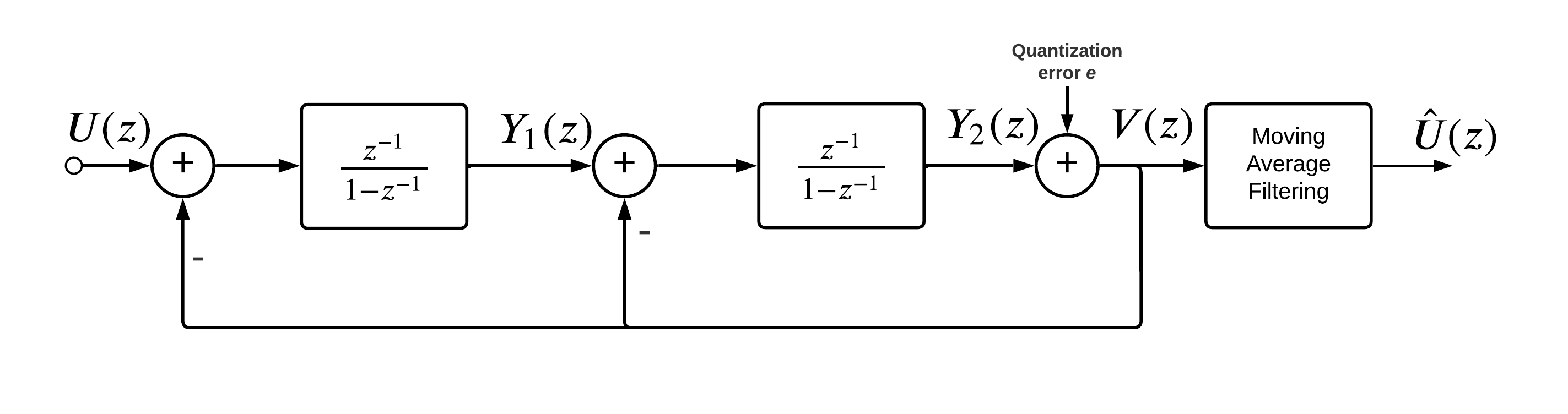
For that, let’s observe the following block diagram of a first order model.
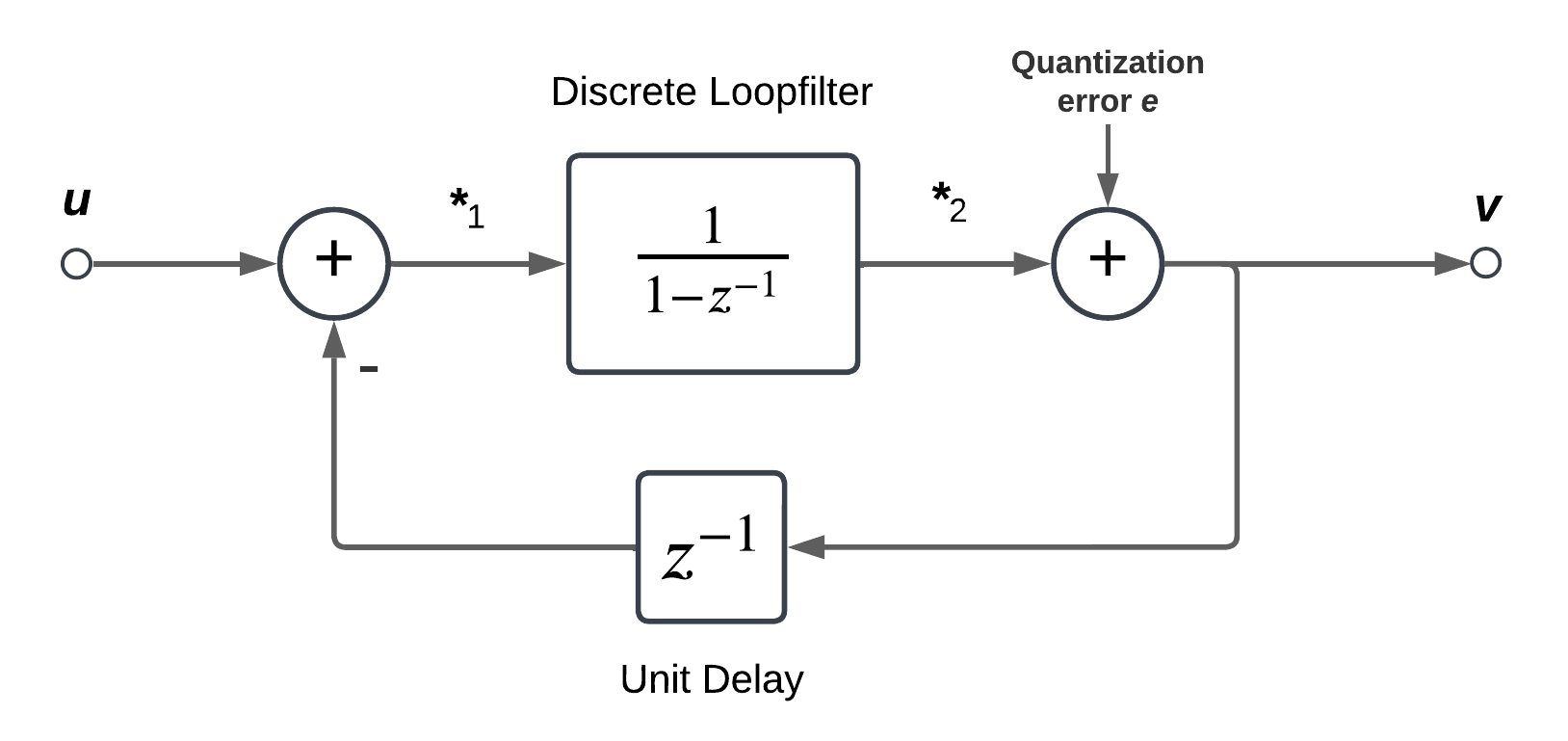
It showcases a simple I/O behavioural model of a system that is inherently representative of what a Delta-Sigma modulator is.
\('U(z)'\) is our input signal, in case of an ADC application it should therefore denote our “analog input”, which we will assume to be handled in a discrete fashion. \('V(z)'\) denotes the output of our feedback system, which should contain sufficient information about our original input, leading to \(\hat{U}(z)\) after the averaging- and decimation process mentioned earlier.
The system contains the so called “loopfilter”, the elemental block for the desired shaping process which is ultimately a delayed discrete integrator, indicating the impact of past samples on the current computation. We also include an additive error, representing the error in our output due to quantization.
Using the markings \(*_1\) and \(*_2\), we can derive the transfer behaviour of our system as follows:
\[\begin{align} V(z) &= E(z) + *_2\,;\quad *_2 = \Big(\frac{z^{-1}}{1-z^{-1}}\Big) \, *_1\,; \quad *_1 = U(z) - V(z)\,z^{-1} \\ \Rightarrow& *_2 = \Big(\frac{z^{-1}}{1-z^{-1}}\Big)\, (U(z)-V(z)\,z^{-1})\\ \Rightarrow& V(z) = E(z) + \Big(\frac{z^{-1}}{1-z^{-1}}\Big)\,(U(z)-V(z)\,z^{-1})\\ \Leftrightarrow&\, V(z) = \frac{U(z)\,z^{-1}}{1-z^{-1}} - \frac{V(z)\,z^{-1}}{1-z^{-1}} + E(z) \\ \Leftrightarrow&\, V(z)\,(1-z^{1}) = U(z)\,z^{-1} - V(z)\,z^{-1} + e(1-z^{-1}) \\ \Leftrightarrow&\, V(z) \cancel{-V(z)\,z^{-1}} \cancel{+ V(z)\,z^{-1}} = U(z)\,z^{-1} + E(z)\,(1-z^{-1}) \end{align}\]
This shows that the output V(z) is comprised of the delay input and the filtered quantization error. We can denote these functions of \(z\) as our transfer functions for either the signal (\(STF(z) = z^{-1}\)) or our quantization “noise” (\(NTF(z) = 1-z^{-1}\))
\[\begin{align} V(z) = STF(z)\,U(z) + NTF(z)\,E(z) \end{align}\]
The noiseshaping is now privided due to the given NTF, which will apply a high-pass characteristic onto the internal quantization noise, with a slope of about 20 dB/decade. As a first general validation of that, if we check over a normalized frequency range of \(\omega = [0, \pi]\) we derive for \(z = e^{j\omega}\) at either z = e^{j} = 1 or z = e^{j} = -1. Plugging that into the proposed NTF will lead to:
\[\begin{align} NTF(z) &= 1-z^{-1} \hat{=} 1-\frac{1}{e^{j\omega}} = 0\,; \quad \text{for}\ \omega \rightarrow 0 \\ NTF(z) &= 1-z^{-1} \hat{=} 1-\frac{1}{e^{j\omega}} = 2\,; \quad \text{for}\ \omega \rightarrow \pi \\ \end{align}\]
Hence, the noise is attenuated for low frequencies, while amplified for high frequencies.
8.2.2 SQNR and ENOB
Having effective noise shaping will increase the Signal-to-Quantazation-Noise-Ratio (SQNR) of the system within the band of interest. The SQNR is fundamentally tied to the “effective number of bits” (ENOB) that can be converted reliably, which is obviously of great interest for our applications.
For a sine wave input to an ideal Nyquist converter, the relation between SNR and the ENOB is given through the following equation, which will serve as our approximation.(Meiners 2024)
\[\begin{align} SNR_{dB} = 6.02 \cdot ENOB + 1.76 \\ \Leftrightarrow ENOB = \frac{SNR_{dB}}{6.02} - 1.76 \end{align}\]
For oversampling circuits, the resulting SQNR of a system is tied to the applied OSR.
In case of the first order system the peak in-band SQNR can be denoted with the following equation
\[\begin{align} SQNR_{1, peak, dB} = 10\,\log \Big(\frac{9\,M^2\, (OSR)^3}{2\,\pi^2}\Big) \end{align}\] where \(M\) indicates the quantizer levels.
The “in-band” region shall be defined from \(\omega = 0\) up to \(\omega = \frac{\pi}{OSR}\). Applying different values for the OSR to this shows, that for each doubling of the oversampling ratio an SNR increase of about 9 dB results.
Using the relation between the SNR and ENOB we can further derive that such an increase in the OSR results in +1.5 effective bits.
Lastly, the topic of stability. The first order model is, in theory, inhereantly stable, due to it’s pole in the very center of the \(z\)-domains unit circle. The only consideration has to be given in the context of the quantizers gain. This however will only result in the condition, that the input has to be chosen bounded, in order to ensure a bounded output (BIBO stability). bounded means, that the input stays within the systems full-scale range (normalized: |u| \(\leq\), ‘1’)
There are more non-ideal aspects to be considered when it comes to the first order \(\Delta\Sigma\) modulator, such as finite accumulator gain, the generation of idle tones or possible deadzones for weak inputs level. We will however not elaborate on those here and instead go over to the topic of increasing our models order.
8.2.3 2nd-Order Modulator Extension
A fundamental second order \(\Delta\Sigma\) modulator can be realized by simply exchanging the quantizer of the first order system with yet another instance of the first-order system. This is an alternative way of increasing the in-band noise suppression instead of utilizing more quantizer levels.
The Blockdiagram will end-up like in Figure 8.4.
Regarding the noise shaping we will ultimately end up with \[\begin{align} NTF_2(z) &= (1-z^{-1})^2 \\ & = 1 - 2\cdot z^{-1} + z^{-2} \end{align}\] , so the square of the previous NTF.
From that we can see that by making this substitution, we are reducing the in-band quantization noise further. As typical for 2nd-order filters, we can now expect a slope with an inclide of 40 dB/ decade for the highpass characteristic of the new \(NTF\).
The peak SQNR achievable with a 2nd order structure, dependend on the given \(OSR\), while M denotes the quantization levels, is given by (Schreier 2017):
\[\begin{align} SQNR_{2, peak, dB} = 10\,\log \Big(\frac{15\,M^2\, (OSR)^5}{2\,\pi^4}\Big) \end{align}\]
The in-band noise is proportional to \(OSR^{-5}\) (prev.: \(OSR^{-5}\)). From the equation we can observe that for doubling the OSR we will achieve approximately +15 dB in SQNR, which in turn results in roughly +2.5 ENOB, which are both reasonable increases to the 1st-order case.
The second order model may require non-linear considerations for the quantizers gain, tied to the relationship between the quant. noise and the input amplitudes. More representative estimations would require adjustments to the \(NTF\). Something that might for example be done for the synthesis of NTFs in MATLAB when using functions from the “delsig” toolbox (Schreier 2017).
For a gain of \(k\), we can rewrite the \(NTF_k(z)\) as
\[\begin{align} NTF_k(z) = \frac{NTF_1(z)}{k+(1-k)\,NTF_1(z)} \end{align}\]
The topic of stability generally gains more importance for the MOD2 system, due to the chance of second-order oscillatory behaviour.
This will result in the need to consider further tweaks to ones model to, leading to the consideration of gain coefficients to sections of the model shown in Figure 8.4. The previous “BIBO” stable condition is also more stright, where the input usually has to be bound to less then the systems full-scale range (e.g. < 0.9). (Schreier 2017)
Table 8.1 shows some of the main impacts that the transformation of our system to the one of second order has.
| Aspect | Due to \(2^{nd}\)-Order |
|---|---|
| Noise Shaping | 40dB/dec instead of 20db/dec |
| 2xOSR impact: Noise Reduction | 9dB -> 15 dB |
| 2xOSR impact: Extra ENOB | 1.5 bit -> 2.5 bit |
| Stability | increased risk -> tighter bounds |
| Complexity | more circuitry (+ stability concerns) |
8.2.4 Specifications for the System
To later interface the system in the context of a system-chain, given e.g. by our meassurement system, a few things should be specified about our desired converter system up front, given the now séstablished theory. Among them are for example the following things, mainly related to our expected inputs.
| Parameter | Value |
|---|---|
| Dynamic Range | 16 Bit ~ 98 dB |
| System Order L | 2 |
| Signal Bandwidth f_B | 215 Hz |
| Nyq. Frequency f_N | 430 Hz |
| Sampling Frequency f_s | 220 kHz |
| Oversampling Ratio (OSR) | 512 |
| Samples per Second (SPS_{max}) | 860 |
8.2.5 Behavioural Analysis/ Confirmation using MATLAB
The behavioural analysis in MATLAB starts by setting some specifications for the system, which are the following:
| Parameter | Value |
|---|---|
| Order of modulator | L = 1 or 2 (order) |
| Structure | form = ‘CIFB’ % Cascade of Integrators Feedback; |
| No optimisation | opt = 0; |
| Quantizer level | nLev = 2; |
| Sampling frequency | fs = 220e3; |
| Sampling time | Ts = 1/fs; |
| OSR | M = 512; |
| Sim. length (output samples), FFT points | N = 16*M; |
| Bandwidth | fB = fs/2/M; |
| Number of sinusoids | cycles = 9; |
| Test tone | fx = cycles * fs/N; |
| Signal amplitude | A = 0.8; |
| Time vector | t = Ts * [0:N-1]; |
| Input signal | u = A * sin(2 * pi * fx/fs * [0:N-1]); |
To validate some of the behavioural characteristics, given by the established theoretical concepts, models for the the 1st- and 2nd order modulators were used within MATLAB & MATLAB Simulink. We will mainly focus on the results from the 2nd-order model to keep this section concise
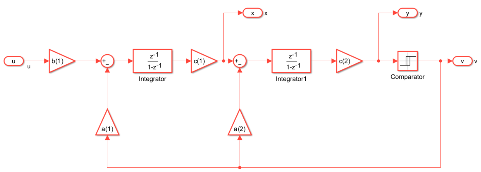
The second order model, as mentioned before, requires tighter bounds, enforced e.g. by gain coefficients which are computed within the initial cells of our MATLAB code, taking into acount the specifications above.
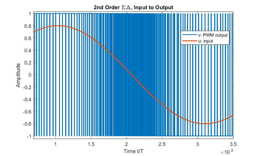
The plot of the model output in the time domain shows the expected indirect representation of the input signal in the momentary duty-cycle of the PMW output, from which one could obtain the input signal by applying a moving average filter to the PMW datastream.
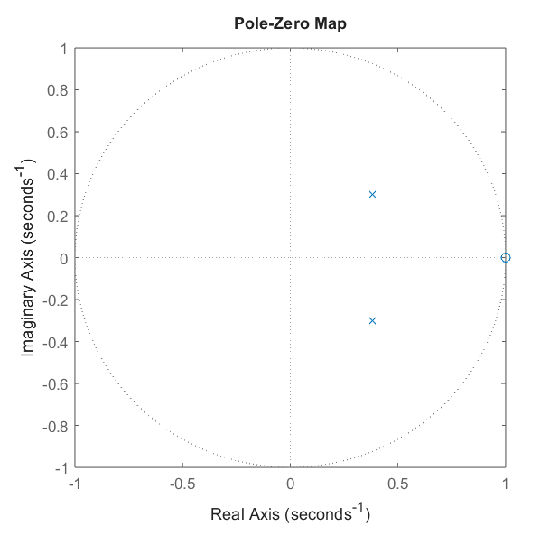
The pole-zero plot from the synthesized NTF object ‘H’ shows the adjusted locations, due to dynamic quantization gain.
MATLAB provides us in this case with an NTF of
\[\begin{align} H = \frac{(z-1)^2}{(z^2 - 0.7639\,z + 0.2361)} \end{align}\]

Lastly, we do observe the expected PSD change betwee the 1st- and 2nd order models, where for the latter the noise power close to dc is lower than for the former, before indicating a slope that is inclining faster (seemingly twice as much, as to be expected) until eventually surpassing the level of the first order PSD. For both cases we observe a signal peak that is clearly separated from the shaped noise power.
9 Basic Behaviour on Circuit Level
In this section, we will deal with realization of our Delta-Sigma Modulator on the circuit level for given specifications. We will consider the basic behaviour of the circuit, and implement them.
The desired loop filter for the modulator, which is the first and most fundamental building block of our system, will be realised utilizing an active integrator circuit that has a switched capacitance input stage.
First of all, let’s see conceptually simplest Sample and Hold (S/H) consists of a Switch and Capacitor in Figure 9.1.

If the Switch is closed, the Capacitor will charge up to the input voltage which denotes to track phase. When Switch is opened, the Capacitor will hold the input voltage which denotes to hold phase, such circuits are also known as Track and Hold circuits.
9.1 Non-Idealities
Unlike ideal Switches, real switches have some On-Resistance \(R_{on}\) which is some function of input. \(\frac{1}{R_{onC}}\) is the bandwidth during the tracking phase. The signal is being stored in Capacitor in terms of charge, smaller the Capacitor more the tendency of getting disturbed or leakage.
Taking a closure look, Resistance is much suspectable to thermal noise and is modelled as voltage \(V_n\) in series with resistance. Ouput Noise is present for all frequencies also known as White Noise and is given as
\[ V_\mathrm{n}^2 = \frac{k T}{C} \]
where \(k\) is Boltzmann’s constant, \(T\) is temperature in Kelvin.
Candidate for switch in circuit is MOSFET. Above were the non-idealities present if switch is ON. Even if switch is OFF its far from being ideal. Ideally, it should be open circuit but there is some \(C_{OFF}\) present.
More critical areas are when MOSFET is transitioning from ON to OFF and vice versa, they give rise to Charge Injection. Injected Charge is Non-Linear function of \(V_{in}\). Due to these reasons we are using Bottom Plate Sampling. Instead of sampling directly at top plate, the bottom plate is switched before capturing the sampled value ensuring non distorted output at feedback or top plate capacitor.
9.2 Switched Capacitor Integrator
A classic implementation of realizing an active integrator would be with the opamp circuit using a switch capacitor. However, in IC level implementation we use OTA instead of OpAMP as output resistance of OTA is infinte which benefits us heavily. \(H(z)\) enables us to realize any Discrete Time Transfer Function. There are two types of integrators:
- Delay Free Integrator: This form of integrator include the current sample of the input signal as well. Its transfer function is given as:
\[\begin{align} {H(z)} = \frac{1}{1-z^{-1}} \end{align}\]
- Delayed Integrator: This form of integrator does not include the current sample of the input signal. Its transfer function is given as:
\[\begin{align} {H(z)} = \frac{z^{-1}}{1-z^{-1}} \end{align}\]
We will be using the second form of integrator in our system.
Therefore, for our desired discrete integrator, it is worth utilizing the following input structure in Figure Figure 9.2, which leads to a switched-capacitor integrator.

The depicted switches are clocked in a way to ensure non-overlapping high levels. This is of great importance, since turning both switches marked as \(\phi_1\) off simultaneously would result in part of the channel charge of the series transistor transfering to the sample capacitor. Since this channel charge is signal dependent, it is nonlinearly related to the input signal. If however the series transistor is still on when turning off the parallel transistor, only a fixed amount of charge is added which introduces a dc offset. (Schreier 2017)
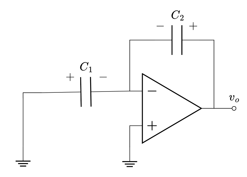
To derive the system behaviour of this circuitry, let’s consider the two phases of operation, given be the switching phases, depicted in Figures Figure 9.3 and Figure 9.4.
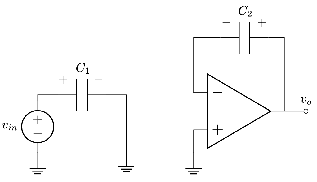
The first phase allows for the capacitor \(C_1\) to be charged from the input, leading to the charge accumulation \(q_1[1]\), during which the integrating capacitor \(C_2\) holds it’s previous charge (\(q_2[n]\)). Due to the relation \(V = \frac{Q}{C}\), the output voltage will be equal to the ratio of that charge \(q_2[n]\) to the capacitance \(C_2\).
The second phase will than result in the charge of \(C_1\) to accumulate in \(C_2\), due to the opamps input behaviour related to it’s “virtual ground”. C2 will therefore have the sum of charges, leading to
\[\begin{align}\label{sc_charge_ph2} q_2[n+1] = q_2 + q_1. \end{align}\]
After applying the \(z\)-transform, the result is
\[\begin{align} Q_2(z) = Q_2(z)\,z^{-1} + Q_1(z)\,z^{-1} \end{align}\]
which in turn can be rearranged to get
\[\begin{align} \frac{Q_2(z)}{Q_1(z)} = \frac{z^{-1}}{1-z^{-1}} \end{align}\]
Utilizing the aforementions relation between voltage, charge and capacitance, we can derive the voltage I/O behaviour (transfer function) to be the following
\[\begin{align} \frac{V_{out}}{V_{in}} = \frac{z^{-1}}{1-z^{-1}} \frac{C1}{C2} = H_v(z) \end{align}\]
The ratio of the capacitors would be a potential gain factor for the, which could also be choosen to achieve unity gain (\(C_1 = C_2\)).
The remaining term, describing a delayed integrator, is what will be utilized in the MATLAB assited system analysis. That ultimately leads to the following description of out feedback system, which overlaps with the established linear model from our system analysis in MATLAB, previously shown in Figure 8.3.
9.3 Ideal system model in LTSpice
For first simulation results the behaviour described in the previous subchapter can be implemented as an indealized model in LTSpice. Files for this were provided by the supervising professor and will be explained briefly.
The simulation of the second order idealized \(\Delta \Sigma\)-Modulator (figure Figure 9.5) comprises two casecaded versions of a switched capacitance stage followed by an integrator. The output of the second integrator is fed into the comparator, whose output is fed back through an inverter to both switched capacitor stages. The second sampling stage is responsible for correctly adding the delayed sample to the output sample of the first integrator.
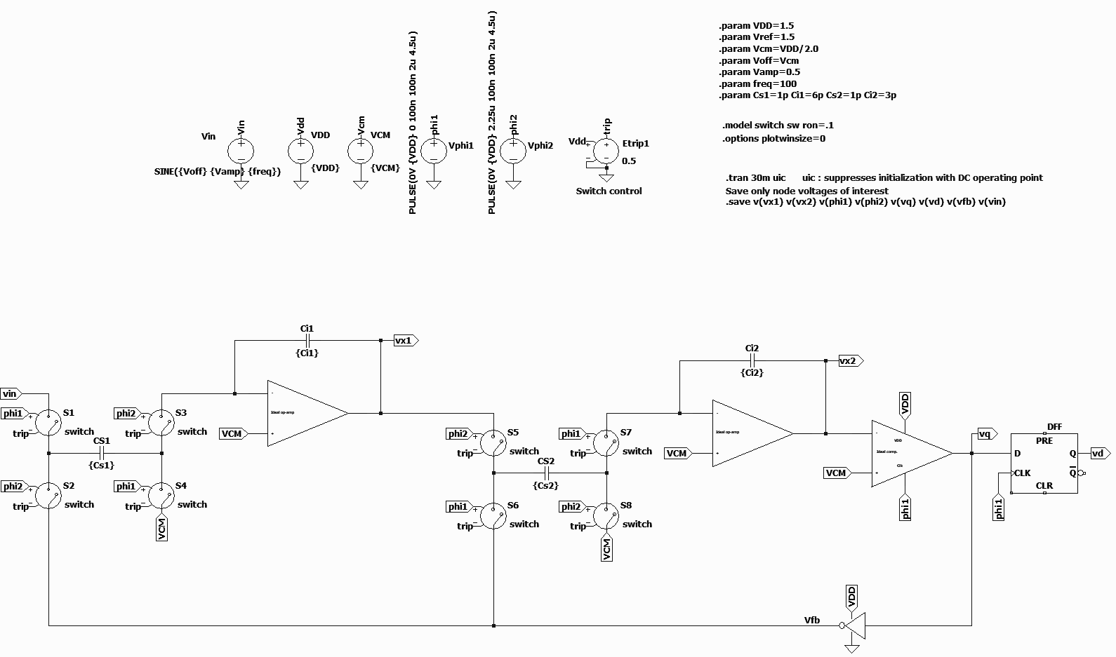
For the input stage, ideal switches are used which are controlled by voltage sources modeling the 220kHz input clocks. These are configured in such a way, that the clock phases are not overlapping. As explained earlier, this is needed to prevent corruption of the sampled signal.
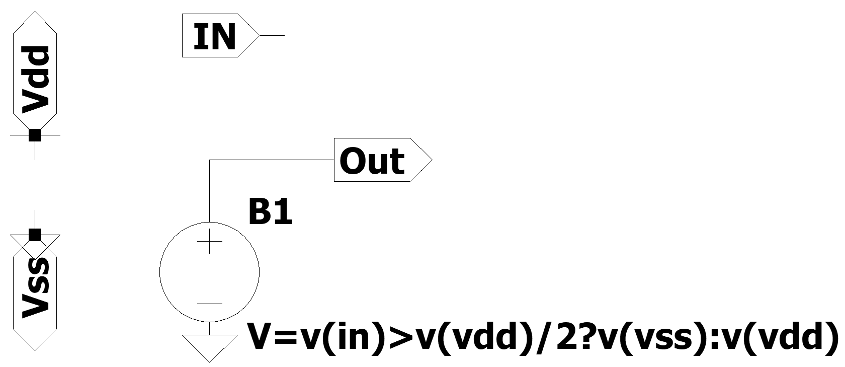
The operational amplifier is is planned to be an operational transconductrance amplifier (OTA) which is realized as a voltage controlled current source that outputs a current proportional to the difference of its two input signals. A parallel resistor creates a corresponding voltage drop. This representation is linear for all inputs and can be chosen, if the input signal can is guaranteed to be within the linear range of the real OTA. If the OTA is to operate in saturation, this model would not be valid anymore.
The comparator has to compare the current input sample to a fixed value. If, at the rising edge of the reference clock, the input voltage lies above this threshold a logic high, represented by \(V_{DD}\) is output, if the value lies below the threshold a logic low (\(V_{SS}\)) will be output. Additionally, this output value has to be held until the next rising edge of the controlling clock. This latching functionallity is realized using two clock controlled switches that open and close inversely. The comparison for the dermination of the output is done through a voltage source and a mathematical comparison.
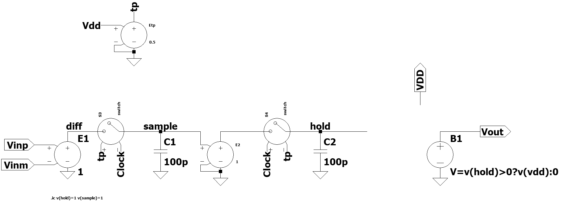
The delay of the comparator output fed back into the switched capacitor stages is realized through an inverter. This is possible, since due to the high sample frequency of the comparator, the width of two successive pulses can be assumed to be very small. Thus, inverting the signal is equal to a delay by one sample. The inversion is again done by a mathematical comparison.
10 Design Proposals
This chapter shall highlight our attempts at realizing the desired subsystems of the \(\Delta\Sigma\) modulator on transistor level, utilizing the 130 nm technology offered from the IHP’s sg13g2 BiCMOS PDK for open source usage.
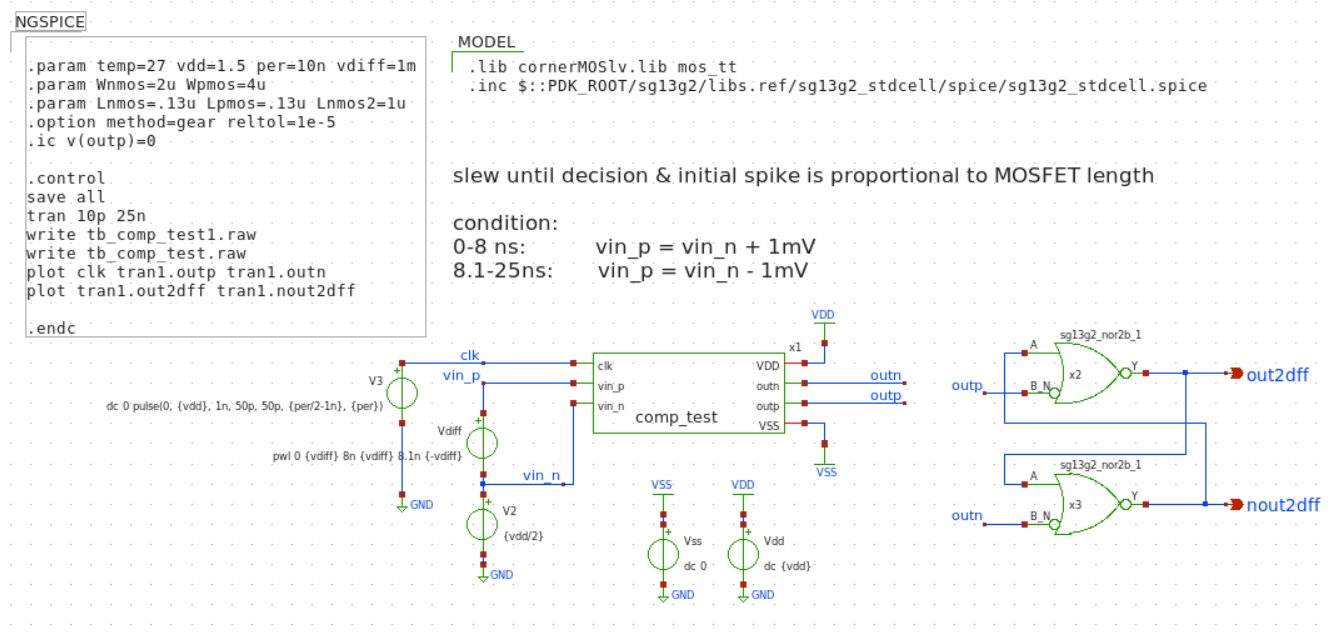
The following subchapters will elaborate on the separate subcircuits, briefly explain the workings of the circuits before going over the achieved simulation results. Xschem was used as the schematic capture EDA tool, while the testbench-driven simulations utilize ngspice.
| Component | Device Name | Specifications |
|---|---|---|
| Low-voltage (LV) NMOS | sg13_lv_nmos |
operating voltage (nom.) \(\VDD=1.5\,\text{V}\), \(L_\mathrm{min}=0.13\,\mu\text{m}\), \(\Vth \approx 0.5\,\text{V}\); isolated NMOS available |
| Low-voltage (LV) PMOS | sg13_lv_pmos |
operating voltage (nom.) \(\VDD=1.5\,\text{V}\), \(L_\mathrm{min}=0.13\,\mu\text{m}\), \(\Vth \approx -0.47\,\text{V}\) |
| High-voltage (HV) NMOS | sg13_hv_nmos |
operating voltage (nom.) \(\VDD=3.3\,\text{V}\), \(L_\mathrm{min}=0.45\,\mu\text{m}\), \(\Vth \approx 0.7\,\text{V}\); isolated NMOS available |
| High-voltage (HV) PMOS | sg13_hv_pmos |
operating voltage (nom.) \(\VDD=3.3\,\text{V}\), \(L_\mathrm{min}=0.45\,\mu\text{m}\), \(\Vth \approx -0.65\,\text{V}\) |
| Silicided poly resistor | rsil |
\(R_\square=7\,\Omega \pm 10\%\), \(\text{TC}_1=3100\,\text{ppm/K}\) |
| Poly resistor | rppd |
\(R_\square=260\,\Omega \pm 10\%\), \(\text{TC}_1=170\,\text{ppm/K}\) |
| Poly resistor high | rhigh |
\(R_\square=1360\,\Omega \pm 15\%\), \(\text{TC}_1=-2300\,\text{ppm/K}\) |
| MIM capacitor | cap_cmim |
\(C'=1.5\,\text{fF}/\mu\text{m}^2 \pm 10\%\), \(\text{VC}_1=-26\text{ppm/V}\), \(\text{TC}_1=3.6\text{ppm/K}\), breakdown voltage \(>15\,\text{V}\) |
| MOM capacitor | n/a | The metal stack is well-suited for MOM capacitors due to 5 thin metal layers, but no primitive capacitor device is available at this point. |
10.1 Clock-Phase generation
The aforementioned delay in the phases of the clocks acting on the switched capacitor can be achieved by the structure in Figure 10.1. This takes a reference clock signal which provides a signal at the frequency required by the system and outputs four different phases \(\phi_1\), \(\phi_{1d}\), \(\phi_2\) and \(\phi_{2d}\). The feedback between the upper and lower strand of the structure, in conjunction with the NAND gates, ensures the prevention of overlap between \(\phi_1\) and \(\phi_2\) and in turn for their respective delayed versions.

By changing the capacitance of the marked inverters the actual delay between \(\phi_i\) and \(\phi_{id}\) can be controlled. (Schreier 2017) It is worth noting however, that the capacitive load \(C_L\) experienced at the outputs of the structure also has an influence on the phase delay.
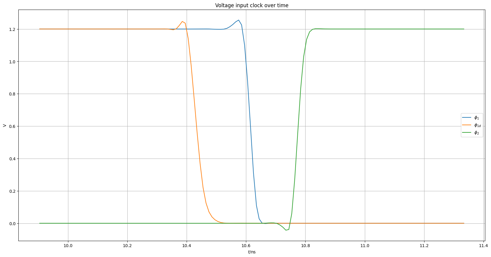
Figure 10.2 shows the normal delay between \(\phi_1\) and \(\phi_{1d}\) as well as the non-overlap with \(\phi_2\). The structure used for clock generation was modeled after the circuit provided by (Murmann 2024). In this, they used the sg13g2 standard cells for the NAND gates and inverters which are not built from single transistors and hence their capacitance can not be changed. Simulations with different values for the load capacitances have proven to not impair the structures functionality. We thus continue with this non-transitorized version, since creating the gates from scratch would add unnecessary complexity.
11 Switch Capacitor Design
We are using “CIFB” topology also known as Cascade of integrators, feedback form to realize our design.
Functions of \(\Sigma \Delta\) toolbox in MATLAB enables us to realize the NTF function and based upon that we can get our coefficients.
11.1 Capacitor Sizing
As mentioned above, the coefficients translate into capacitor ratios. In the first stage capacitance ratio can be computed as follows:
\[ a_1 = \frac{C_1 V_\text{ref}}{C_2} = \frac{C_1 V_\text{dd}}{C_2} \]
\[ b_1 = \frac{C_1 V_\text{FS}}{M C_2} = \frac{C_1 V_\text{dd}}{C_2} \]
The absolute value of \(C_{1}\) is computed by thermal noise constraint. Mean-square noise yielding an SNR of 101 dB is
\[ \overline{v_n^2} = \frac{\left(\frac{V_\text{dd}}{2}\right)^2 / 2}{10^{\text{SNR}/10}} \]
The in-band input-referred mean-square noise voltage associated with first integrator:
\[ v_n^2 = \frac{kT}{\text{OSR} \cdot C_1} \]
From above equations we can get the value of \(C_1\) and \(C_2\). For capacitences for the second integrator can be computed from:
\[ c_1 = \frac{C_3}{C_5} \]
\[ a_2 = \frac{C_4 V_\text{dd}}{C_5} \]
Since, due to oversampling ratio is high, the in-band thermal noise of the second integrator is heavily attenuated by gain of the first integrator. Therefore, we set \(C_4\) is taken 0.1pF.
11.2 OTA Sizing
For integrator, we first implemented 5 transistor OTA. Using components available in IHP Microelectronics SG13G2 technology. First of all, we need to run the technology sweep to get the response of the OTA at various \(V_{gs}\) and \(V_{ds}\) values. Then we can use the sweep data to get the optimal graphs in MATLAB.

We have a similar tesbench for LV_PMOS which to depict their behaviour. We would use the data provided by these sweep to realize the sizing of OTA discussed below Figure 11.2

11.2.1 Choosing \(I_{d}\) and \(g_{m}\)
The value of \(I_d\) plays a very important role in the design of the OTA. At the start of each charge-transfer phase, the OTA input terminals are driven such that current in differential switches fully to one side. The magnitude output current of I (bias current) in each half of differential pair. It should be large enough to transfer the charge from input capacitor to integrating capacitor in allowed time.
\[I > \frac{C_1 V_\text{dd}}{T / 4}\]
Next important parameter is \(g_m\).In small-signal model of an integrator in charge-transfer phase from which we can see time-constant is
\[ \tau = RC = \frac{C_1 + C_3 + C_1C_3 / C_2}{g_m} \]
which gives
\[ g_m = \frac{C_1 + C_3 + C_1C_3 / C_2}{T/48} \]
Now, we have both the values of \(I_d\) and \(g_m\). We would divide the two values to get \(g_m/I_d\) ratio and check whether it is in moderate region or not. If it is not, we need to adjust the value of \(I_d\) and \(g_m\) which can be done by increasing the value of \(I_d\).
11.2.2 Choosing W and L parameters
In a design we would have different NMOS and PMOS with different parameters depending upon their presence in design. We have used Whilson Current Mirror for creating reference current in our circuit. All NMOS and PMOS in this section would have double \(W/L\) compared to the NMOS and PMOS in the differential pair.
We would generate MATLAB scripts or also known as lookup table to generate the required plots for our technology node. In figure \(g_m/I_d\) vs \(I_d/W\) for NMOS. We can see that \(g_m/I_d\) is in moderate region and for various \(L\) values corresponding \(I_d/W\) values can be see. Choose the length value in such a way that after calculation your \(W\) is not less 130nm. Repeat the same procedure for PMOS. You have \(W\) and \(L\) values for both NMOS and PMOS but keep in mind choose length atleast three or four times of \(L_{min}\). We get similar graph attached below for PMOS as well.

11.3 Xschem Realization
To simulate our design we are using Xschem and ngspice. Realization of Telescopic OTA as after Figure 11.2 was not compatible with Switched Capacitor. 


Its giving us DC Gain of 9.6059e-01, Gain error of -3.9408e-02 and Slew rate (\(t_{settle}\)) of 7.0329e-07 at \(I_0\) equivalent to 0.8microA.Below is the Switch Capacitor circuit with phase 1 and 2.

11.4 Comparator Design
As the output stage of the modulator subsystem of the desired \(\Delta\Sigma\) modulator, the comparator stage serves to realize the desired quantization to discretize the amplitude of our analog signal. A comparator suffices to realize a 1-bit quantization, where the representative output from our data samples is either “high” or “low”, which will do fine to give us the PWM signal at the output.
11.4.1 Model-/ Architecture elaboration
The considered implementation of our comparator utilizes an initial inverter based comparator stage, followed by a latching circuit to account for the reseting within the comparator and the resulting “invalid” outputs it would provide. Lastly we could consider utilizing a d-flip-flop for the “digitized” output signal(-s), also to be fed back to the loopfilter structures.
11.4.2 Comparator Stage
The inverter-based comparator structure is realized through a symmetric architecture that is closely assossiated to the so called “StrongArm” architecture, depicted in Figure 11.5.
While the classical StrongArm would utilize pmos transistors for M3 & M4 (with their sources being pulled to \(V_{DD}\) and their drains connected to the node above M1 and M2) instead, the behaviour would in both cases be the same, as tested in simulations.
It utilizes both n- and pmos transistors that are generally sized with small values for L, due to the main usage as switches.

(to be cited:
- Low Voltage, Low Power, Inverter-Based Switched-Capacitor Delta-Sigma Modulator
- Murmann lectures (e.g. 6) )
This circuits behaviour is fundamentally tied to the clock states, leading to either the so called “precharge” phase during low clock levels, or the “amplification” phase during an active clock phase.
During low clock phases the pmos transistors, directly tied to the supply rail, open up and therefore pull both the output nodes to \(V_{DD}\), charging the internal capacitances of the structure.
During high clock phases the nmos transistors (above the input nmos transistors) start to conduct and allow for current to flow to the shared source contact of the input differential pair, so to \(V_{SS}\)
Depending on the conductivity of the MOSFETS that are fed by the input signals, one branch will “discharge” quicker. This in turn will lead to either M7 or M8 conducting again, once the applied gate voltage drops below the \(V_{DD}-V_{th}\) (since they are pmos). So, in case of \(in+ > in-\), the gate of M8 would reach that level faster, therefore conducting earlier and in the process pulling outp back to \(V_DD\), while this in turn ultimately negates M7 from reaching that level, leading to outn decaying further to \(V_{SS}\).
11.4.3 Latching Circuit
After the StrongArm comparator, as mentioned previously, a latching circuit is implemented for improved validity of the final outputs. The way this was done in our case is through an “SR-Latch”, which stands for “set” and “reset”.
In general, such a latch utilizes two logic gates with 2 inputs and one output each, where one of the inputs will be one of the input signals, while the other will be the fed-back output signal from the respective other logic gate. The provided logic should result in only the Q output or it’s complement nQ to be high, depending.
The main task of this block is to only change it’s output, while either the positive or negative output of our comparator is “high”. For SR-latches there will be one case for equal inputs (either both “high” or both “low”) where one will not result in a change to the output while the other will ultimately result in an output, where the intended logic of the circuit is violated. With the chosen NOR gates (including inverted inputs) depicted in Figure 11.6, that violation would occur for a high level on both inputs, which is not given due to the StrongArm comparators operation paired with the inverters.
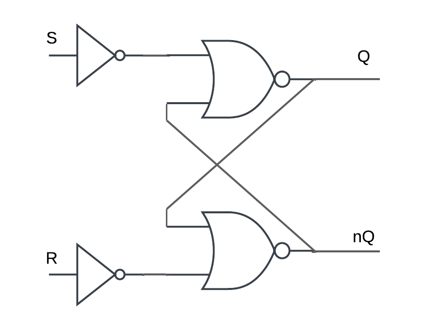
Therefore, this logic block should change with each positive clockphase where either S (outp) or R (outn) will be high, while keeping that state during the negative clock phases where both outp and outn are “high”.
11.4.4 Implementation
The comparator is realised in the following way

This circuit is proposed by Boris Murmann in his EE628 lecture series (e.g. lec 6, (Murmann 2024)), while he himself adopted the design from the paper given in (Chae and Han 2009). The MOSFET lengths (L) can be chosen minimal (\(\approx\) 130 nm), since almost all of them simply serve as switches, with only those for the inputsignal are choosen with a slightly greater margin.
While the mentioned sources also propose a latching circuit, we will directly utilize the logic gates available through the used PDK, which generally helps to make the comparator system more universally applicable. Specifically, the proposed design showed a lesser tolerence for very small differences between the input signals, once the latch was cascaded. This becomes worse for higher supply voltages (e.g. 3V3 instead of 1V5).
The testbench file is shown next in Figure 11.8.
11.4.5 Validation
The following plots show the outputs of both the comparator and the cascaded SR-latch. For the first 8 ns, the positive input voltage of the comparator is 1 mV higher than the negative input. At around 8.1 ns, that polarityis reversed.
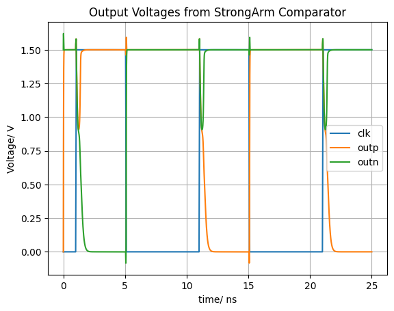
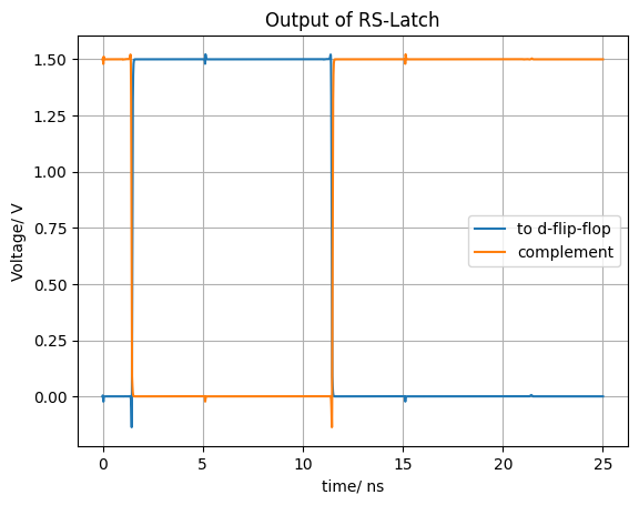
A clock period of 10 ns is chosen, which is much shorter then for our actual application. Therefore proving, that even for a fraction of the desired clock period, the circuit is sufficiently fast when it comes to settling. The latch outputs show the desired behavior, where only during the active clock periods the output will change in case the polarity of the input difference has changed, while remaining constant during the reseting of the comparator.
The output “out2dff” can now be forwarded to a d-flip-flop, which most comparator designs for ADCs would utilize to gain the “final” clk-controlled digitized output sample.
The behavior is the pretty much the same, both for \(V_{DD}\) equaling 3.3 V or 1.5 V, where only the small spikes on the latch output are smaller for 3.3 V.
The designs that are considerable as the final results are given within our design directory with “final_working_comp.sch”, “latched_comp.sch” and “latched_comp_dff.sch”, the latter also including a d-flip-flop based on design objects PDK.
12 Digital Section
The PWM signal output by the comparator represents the input signal but also the quantization error. Thanks to the noise shaping, this error is found at higher frequencies. By applying a lowpass filter, one can reduce this error while retaining the original signal. The requirements for this lowpass filter can be quite strict thus requiring a high order digital filter. With the high frequency error removed, the signal still possesses a high sample rate. However, these samples do not carry additional information, their number can be reduced due to the nyquist theorem. (Schreier 2017) (Baker 2011) This allows the output data rate of the decimator to be much lower and thus relaxes the speed requirements for the following processing unit.
Conceptually, the digital section can be represented as seen in figure Figure 12.1. The signal is lowpass filtered and then decimated for a significantly lower output data rate.

The high oversampling ratio of \(M = 512\), together with the tight transition band of the filter, increases the computational complexity. In MatLab, the decimation can be done by use of the decimate function. This takes the signal to be downsampled, as well as the downsampling factor, automatically creates a lowpass Chebyshev Type 1 IIR filter and returns the decimated signal. The result can be observed in figure Figure 12.2.
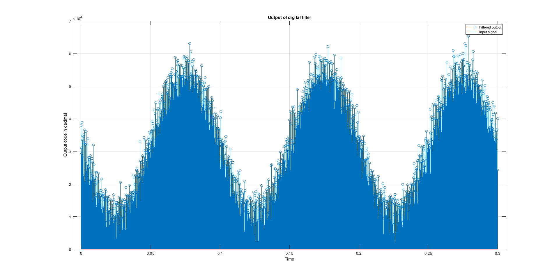
As can be seen, this signal is quite noisy. This can be attributed to poor filtering. Unfortunately, due to timing reasons the proper filtering using an FIR filter could not be further explored. It is however noteworthy, that the use of an IIR filter is generally not recommended. The use of FIR filters leads to a factor of \(M\) savings in the computaional complexity. Assume the structure in figure Figure 12.1, where \(H_d(z)\) is a length-N FIR filter with
\[\begin{equation} v[n] = \sum_{m=0}^{N-1} h[m]x[n-m] \end{equation}\]
The down-sampler only keeps every M-th sample of v[n], hence it is sufficient to only compute v[n*M], skipping the computations in between.
Due to the feedback structure inherent to IIR filters however, where
\[\begin{equation} H_d(z) = \frac{\sum_{n=0}^Kp_nz^{-n}}{1+\sum_{n=1}^Kd_nz^{-n}} \end{equation}\]
the feedback signal \(w[n]\) must be computed for all values of \(n\). Therefore, the savings are always less than \(M\). (Wolter 2025)
13 Conclusion
This marks the end of the design document. We have explored the basic theoretical aspects of \(\Delta\Sigma\)-ADC’s and proposed our design ideas regarding a custom modulator, including a five transistor OTA as the loop filter. We have also presented corresponding simulations showing promising results. Despite all, there is still a lot of work left, mainly in the area of integrating the singular subsystems, like the OTA, the switched capacitor and the clock generator. Furthermore, the subject of digital filtering needs further exploration, as no real design proposal could be made, due to time limitations.
References
Alan Doolittle. 2025. “Lecture 25 - MOSFET
Basics (Understanding with Math.” https://alan.ece.gatech.edu/ECE3040/Lectures/Lecture25-MOSTransQuantitativeId-Vd-Vg.pdf.
Allelco. 2025. “Schmitt Triggers in Modern
Electronics: Understanding Their Role and Capabilities.”
https://www.allelcoelec.com/blog/schmitt-triggers-in-modern-electronics-understanding-their-role-and-capabilities.html.
Bajdechi, Ovidiu. 2004. “Systematic Design of Sigma-Delta
Analog-to-Digital Converters.” In Analog Circuit Design:
Sensor and Actuator Interface Electronics, Integrated High-Voltage
Electronics and Power Management, Low-Power and High-Resolution
ADC’s, edited by Michiel Steyaert, Arthur H. M. van Roermund, and
Herman Casier, 293–326. Springer. https://doi.org/10.1007/978-1-4020-7997-5_13.
Baker. 2011. “How Delta-Sigma ADCs Work, Part 1.”
Analog Applications 7.
Baker, Bonnie. 2011. “How Delta-Sigma ADCs Work, Part 2.”
Analog Application Journal (AAJ).
Baker, R. Jacob. 2008. CMOS: Circuit Design, Layout, and
Simulation. Wiley-IEEE Press. https://www.wiley.com/en-us/CMOS%3A+Circuit+Design%2C+Layout%2C+and+Simulation%2C+3rd+Edition-p-9780470290260.
Boris Murmann. 2016. “Systematic Design of
Analog Circuits Using Pre-Computed Lookup Tables.” https://www.ieeetoronto.ca/wp-content/uploads/2020/06/20160226toronto_sscs.pdf.
———. 2024. “EE 628 - University of Hawai’i as
Manoa, Analysis and Design of Integrated Circuits.” https://github.com/bmurmann/EE628/tree/main/1_Lectures.
Boser, B. E., and B. A. Wooley. 1988. “The Design of Sigma-Delta
Modulation Analog-to-Digital Converters.” IEEE Journal of
Solid-State Circuits 23 (6): 1298–308. https://doi.org/10.1109/4.90025.
Chae, Youngcheol, Jimin Cheon, Seunghyun Lim, Minho Kwon, Kwisung Yoo,
Wunki Jung, Dong-Hun Lee, Seogheon Ham, and Gunhee Han. 2011. “A
2.1 m Pixels, 120 Frame/s CMOS Image Sensor with Column-Parallel ΔΣ ADC
Architecture.” IEEE Journal of Solid-State Circuits 46
(1): 236–47. https://doi.org/10.1109/JSSC.2010.2085910.
Chae, Youngcheol, and Gunhee Han. 2009. “Low Voltage, Low Power,
Inverter-Based Switched-Capacitor Delta-Sigma Modulator.”
IEEE Journal of Solid-State Circuits 44 (2): 458–72. https://doi.org/10.1109/JSSC.2008.2010973.
Clifford, Michael. 2016. “Fundamental Principles Behind the
Sigma-Delta ADC Topology: Part 1.” Analog Devices (AD). https://www.analog.com/en/resources/technical-articles/behind-the-sigma-delta-adc-topology.html.
Devices, Analog. 2010. Small, Low Power, 3-Axis ±3 g
Accelerometer. Analog Devices.
Dobkin, Bob, and Jim Williams. 2011. Analog Circuit Design: A
Tutorial Guide to Applications and Solutions. Elsevier/Newnes. https://www.elsevier.com/books/analog-circuit-design/dobkin/978-0-12-385185-7.
Dr. Andrew Masami Abo. 1992. “Design for
Reliability of Low-voltage, Switched-capacitor Circuits.”
https://designers-guide.org/forum/Attachments/SC_Dissertation.pdf.
Filanovsky, M., and H. Baltes. 2004. “Theory and Applications of
Incremental ΔΣ
Converters.” IEEE Transactions on Circuits and Systems-1:
FUNDAMENTAL THEORY AND APPLICATIONS 41 (1): 46–49. http://web.mit.edu/magic/Public/papers/00260219.pdf.
Fraden, Jacob. 2015. Handbook of Modern Sensors. Springer
International Publishing Switzerland. https://doi.org/https://doi.org/10.1007/978-3-319-19303-8.
G. Jovanovic, Mile Stojcev, and Zoran Stamenkovic. 2010. “A CMOS
Voltage Controlled Ring Oscillator with Improved Frequency
Stability.” Scientific Publications of the State University
of Novi Pazar Series A Applied Mathematics Informatics and
Mechanics 2 (0): 1–9. https://www.researchgate.net/publication/266265623_A_CMOS_Voltage_Controlled_Ring_Oscillator_with_Improved_Frequency_Stability?enrichId=rgreq-ea65c1847781412dd1f866311352b440-XXX&enrichSource=Y292ZXJQYWdlOzI2NjI2NTYyMztBUzoxNDc0MTUzNDA0MjUyMTdAMTQxMjE1Nzk2NDc3NA%3D%3D&el=1_x_3&_esc=publicationCoverPdf.
Gift, Stephan J. G. and Maundy, Brent. 2022. “Operational
Amplifiers.” In Electronic
Circuit Design and Application, 325–73. Cham: https://doi.org/10.1007/978-3-030-79375-3_8;
Springer International Publishing. https://doi.org/10.1007/978-3-030-79375-3_8.
Goldenbaum, Prof. Dr.-Ing. Mario. 2022. “Grundlagen Der
Informationstechnik.”
H. Pretl. 2025. “IIC-OSIC-TOOLS.” https://github.com/iic-jku/IIC-OSIC-TOOLS.
H. Pretl and Michael Koefinger. 2025. “Analog Circuit
Design.” https://iic-jku.github.io/analog-circuit-design/.
IHP. 2025. “SiGe BiCMOS and Silicon Photonics
Technologies.” https://www.ihp-microelectronics.com/services/research-and-prototyping-service/mpw-prototyping-service/sigec-bicmos-technologies.
IHP GmbH. 2025. “MPW-Zeitplan 2024 & 2025
und Preisinformationen 2024.” https://www.ihp-microelectronics.com/de/leistungen/forschungs-und-prototyping-service/mpw-prototyping-service/zeitplan-preisliste#c1379.
Instruments, Texas. 2009. ADS111x Ultra-Small, Low-Power,
I2C-Compatible, 860-SPS, 16-Bit ADCs with Internal Reference,
Oscillator, and Programmable Comparator. SBAS444D ed. Texas
Instuments.
Kester, Walt. 2005. The Data Conversion Handbook. Burlington,
MA: Newnes/Elsevier.
Markus, J., J. Silva, and G. C. Temes. 2004. “Theory and
Applications of Incremental ΔΣ Converters.”
IEEE Transactions on Circuits and Systems I: Regular Papers 51
(4): 678–90. https://doi.org/10.1109/TCSI.2004.826202.
Maxim. 2003. “Demystifying Delta-Sigma ADCs.” Tutorial
1870. Maxim Integrated.
Meiners, Mirco. 2024. “CEMS - Lecture 5: Oversampling
ADC’s.”
Meyer, Martin. 2019. Kommunikationstechnik: Konzepte Der Modernen
Nachrichtenübertragung. Wiesbaden: Springer Vieweg.
Mitra, Sanjit K. 2001. Digital Signal Processing: A Computer-Based
Approach. McGraw-Hill Higher Education.
Murmann, Boris. 2024. “EE628.” GitHub. 2024. https://github.com/bmurmann/EE628.
Pavan, Shanthi, Richard Schreier, and Gabor C. Temes. 2017.
Understanding Delta-Sigma Data Converters. IEEE Press Series on
Microelectronic Systems. John Wiley & Sons.
Pretl, Harald, Michael Koefinger, and Simon Dorrer. 2025. “Analog
Circuit Design.” February 2, 2025. https://doi.org/10.5281/zenodo.14387481.
Razavi, Behzad. 2015. “The StrongARM Latch [a Circuit for All
Seasons].” IEEE Solid-State Circuits Magazine 7 (2):
12–17. https://doi.org/10.1109/MSSC.2015.2418155.
Rosa, Jose M. de la. 2011. “Sigma-Delta Modulators: Tutorial
Overview, Design Guide, and State-of-the-Art Survey.” IEEE
Journal of Circuits and Systems 58 (1): 1–21. https://ieeexplore.ieee.org/document/5672380.
Rosa, Jose M. de la, and Rocío del Río. 2013. CMOS Sigma-Delta
Converters: Practical Design Guide. John Wiley & Sons, Ltd.
https://doi.org/https://doi.org/10.1002/9781118569221.
Ross Walker. 2017. “Chapter 5, gm/ID - Based
Design.” https://web02.gonzaga.edu/faculty/talarico/EE406/documents/gmid.pdf.
Schreier, Richard. 2017. Understanding Delta‐sigma Data
Converters. John Wiley & Sons, Ltd. https://doi.org/https://doi.org/10.1002/9781119258308.ch1.
Schreier, Richard, Gabor C Temes, et al. 2005. Understanding
Delta-Sigma Data Converters. Vol. 74. IEEE press Piscataway, NJ.
Silveira, F., D. Flandre, and P. G. A. Jespers. 1996. “A Gm/Id
Based Methodology for the Design of CMOS Analog Circuits and Its
Application to the Synthesis of a Silicon-on-Insulator Micropower
OTA.” IEEE Journal of Solid-State Circuits 31 (9):
1314–19. https://doi.org/10.1109/4.535416.
Williams, Arthur, and Fred J. Taylor. 2006. Electronic Filter Design
Handbook, Fourth Edition. 4th ed. McGraw-Hill Professional.
Wolter, Stefan. 2023. “Digital Signal Processing II – Lecture
Slides.” University of Applied Sciences Bremen. https://wolter.hs-bremen.de/skripte/DSP_II/.
———. 2025. “Digital Signal Process II.”